CN
CN EN
EN


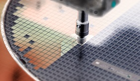
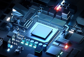
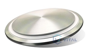
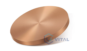
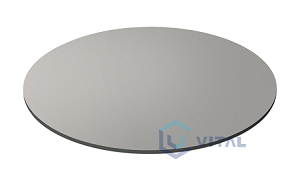
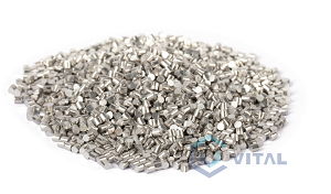
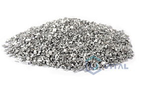
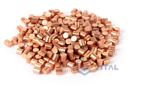
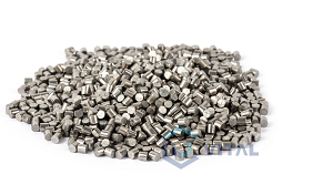
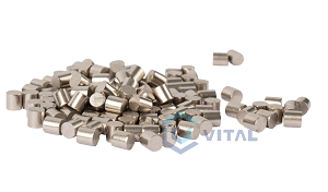
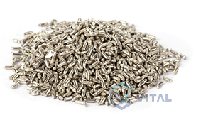
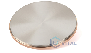
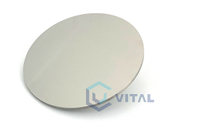
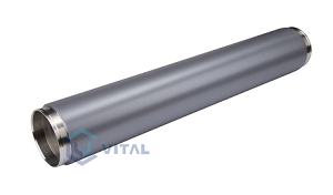
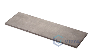
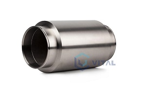
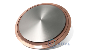
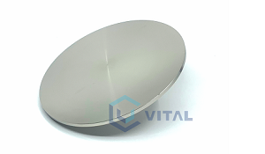
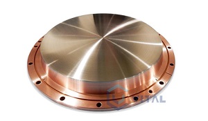
Physical vapor deposition (PVD) sputter targets and evaporation materials are widely used within semiconductor chip fabrication, including front-end and back-end processes. Chip densification is no longer the driving technology for growth, but rather a shift to adding functionality.
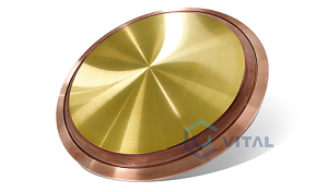
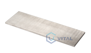
Vital Thin Film Materials (VTFM) is a uniquely positioned supplier of PVD evaporation and sputtering materials. Starting raw materials largely originate from in-house recycling, also referred to as ‘urban mining’. Furthermore, in-house refining, melting, casting, forging, rolling and bonding allow VTFM to have direct control over material attributes (purity, grain size, homogeneity, etc.) critical to the PVD process.
These production resources are equally complimented by an R&D team available to assist customers with process improvements, including new material compositions and geometries or depositing layer stacks within our own applications laboratory.